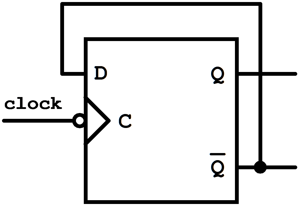
Figure 7.11: D Flip-Flop used as T Flip-Flop.
| Contents | Previous Chapter | Next Chapter |
When the realization of a counter should be done in asynchronous form, an additional design phase between step 1 and step 2 has to be introduced compared to the synchronous design, in order to arrange the clocking of the flip-flops used in this application.
Step 1:
Determination of the required number of Flip-Flops and the State Coding.
This development phase is the same as in the design of synchronous counters.
Step 2: Clock signal generation
For each necessary counting step it has to be determined which flip-flops have to chance their values. Only for these flip-flops a clock signal will be produced. Besides the external clock signal it is also possible at this point to apply suitable changes of flip-flop outputs.
Flip-flops whose outputs remain stable will not be clocked; therefore their logic inputs remain undefined, they can be treated as "don't care" positions. Among other things this leads to considerable simplifications in the combinational circuit.
Thus it is not necessary to select the function "store" for this purpose, as in the case of synchronous counters; with asynchronous counters the same is achieved by "not clocking".
Step 3:
Design of the combinational circuit.
Now the combinational circuit must not only supply the signals to the logic inputs but also to the clock inputs.
Compared to the synchronous circuits the situation becomes confusing, because immediately after a FF change old and new input signals are applied to the network. The new values move through the combinational circuit like a wave, until after several intermediate results finally the next counter value will be available at the output Y.
Hint:
Design Example:
As an example for the design of an asynchronous counter circuit the development of a "Modulo-16 Counter" will be discussed.
Table 7.1: Transition table for the asynchronous mod-16 counter.
For each bit change of a variable now the following consideration will be done:
Does a flip-flop output exist whose signal change based on its switching behaviour can directly be used to clock a state variable?
Obviously the cases exist, some example transitions have been marked in the above table.
Thus for the asynchronous clocking of the Mod-16 counter the following possibilities exist:
| FFA: | this flip-flop changes with every clock signal, consequently it must be controlled by the external clock signal; |
| FFB: | Flip-flop B changes with the transition QA: 1 → 0, hence clocking occurs with QA; |
| FFC: | Flip-flop C changes with the transition QB: 1 → 0,hence clocking occurs with QB; |
| FFD: | Flip-flop D changes with the transition QC: 1 → 0, hence clocking occurs with QC. |
Tab. 7.2: Clock supply for the mod-16 counter.
Figure 7.11: D Flip-Flop used as T Flip-Flop.
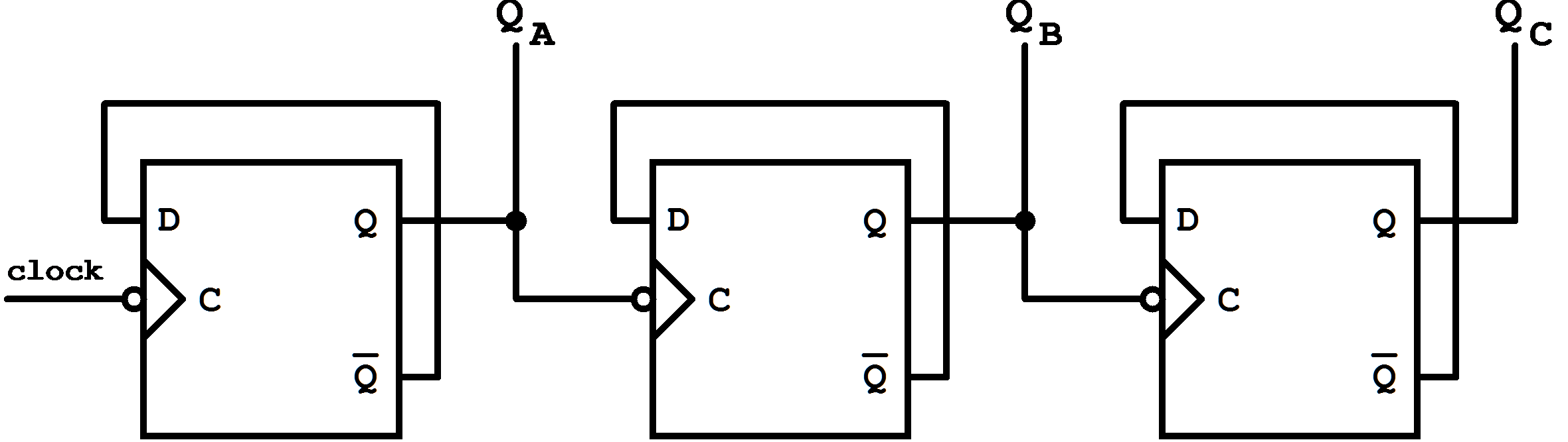
Figure 7.12: Using D Flip-Flops to implement a mod-16 counter.
The BCD counter represents a binary counter that returns to the initial state '0' after reaching the counter result '9'. Therefore it can also be called a
"Modulo-10" counter:
Table 7.3: Transition Table for the asynchronous BCD Counter.
For the states '9' to '15' known from the binary counter, which are not realized in the BCD counter, the term "Pseudo Tetrades" ("Pseudo Decimals" , see also the "Modulo-6" counter) is used.
For the circuit realization especially two solutions are possible, which will both be compared:
7.3.2 BCD Counter as modified Mod-16 Counter
As can be seen from the transition table, the BCD counter is similar to the already treated "Modulo-16" counter. Consequently its clocking can be adopted, but it must be modified when the counter limit, characteristic for the BCB counter, is reached.
For clocking, besides the clocking pulse the "1 → 0" transition of the involved flip-flops should be available (falling edge is active).
|
|
| |||||||
Table 7.4: Transition Table of the asynchronous BCD counter.
Which modifications have to be done to the Mod-16 counter can be seen from the transition table 7.4.
The comparison between the Mod-10 and Mod-16 counter at the counting limit (clock 9) shows that the clocking of FFA and FFC do not have to be changed. For FFB and FFD the following modification has to be built in:
Flip-flop B:
The under normal circumstances occurring transition
0 → 1 must be avoided. This can be achieved by not clocking (the D input could also be set to '0', but that would be untypical for asynchronous counters).
When furthermore the clocking with
CB = QA should be maintained, then it obviously may only occur now as long as QD = 0
Thus the following solution is found for CB:
| . | (7.6) |
Flip-flop D:
Additionally to the clocking with CC, clocking is now needed for the case QA = QD
= 1. Therefore it follows:
| . | (7.7) |
7.3.3 Systematic design as an asynchronous counter
To make a complete design of the asynchronous BCD counter, the first steps are similar to the synchronous case.
In the first step the transition diagram is designed. Four flip-flops are necessary, therefore a K-Map with four variables is chosen. Then the desired counting sequence will be documented:
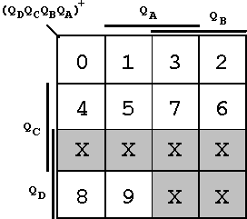
Figure 7.13: Transition Diagram of the BCD counter.
In this diagram the Pseudo Tetrades of the counter are marked a 'X'. These "don't-care" fields are the first positions for a later optimization.
Next the application diagrams are prepared. Corresponding to the transition table in this diagram at first those fields have to be marked for which clocking must occur (i.e. those fields that correspond to a changing signal Q+). About this "necessary" (minimal) clocking can also be decided with the help of the transition table.
| Table 7.5: Necessary Clocking of the asynchronous BCD Counter. |
|
Obviously a clocking scheme using the following (asynchronous) procedure is not possible:
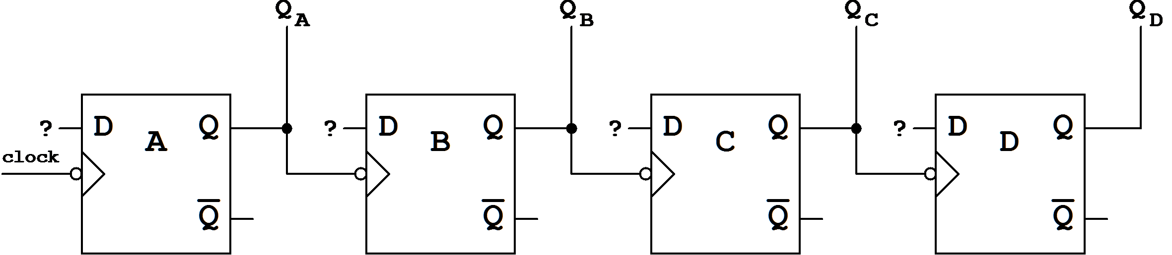
Figure 7.14:
Asynchronous counter setup (ripple-counter).
This circuit does not allow the required clocking of flip-flop D (see transition diagram).
Whereas for flip-flops A, B, and C the clocking shown here can be maintained, flip-flop D must be clocked with QA as can be seen from the table (clocking with the input clock signal could also be done, but this would lead to a higher circuit complexity, see below):
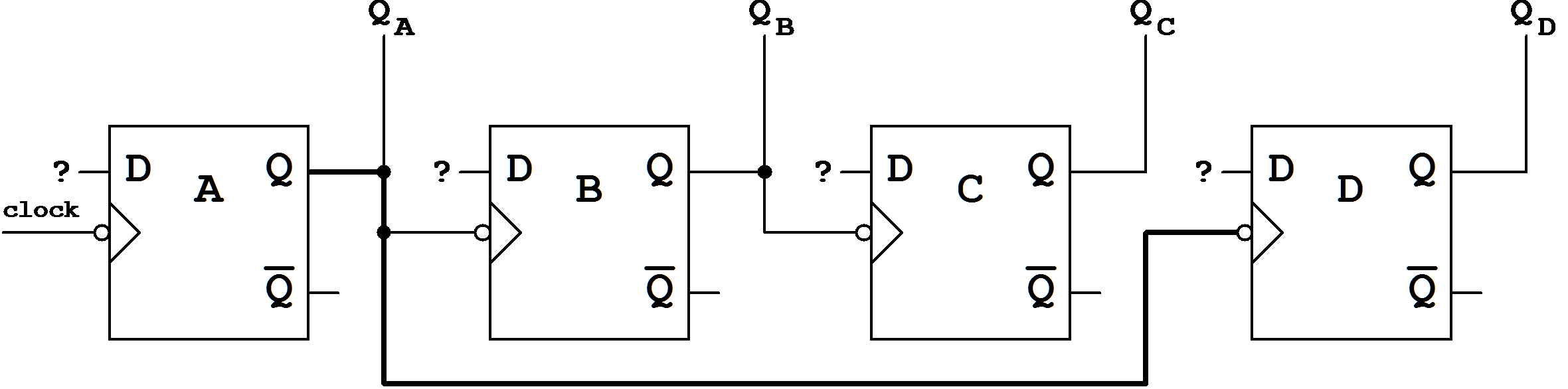
Figure 7.15: Asynchronous counter with modified clocking.
When this basic circuit is chosen it has to be observed that an extended clocking exists. Flip-flop B will be additionally clocked with the state change 9, the same is valid for flip-flop D, which will be additionally clocked by flip-flop A at clock positions 1,3, and 5.
Thus the following clocking has to be considered:
| Table 7.6: Selected clocking of the asynchronous BCD counter (the additional clock signals are indicated in parenthesis.). |
|
In the application diagram (Fig. 7.16) the fields that correspond to those clock positions are marked. Not indicated fields can be considered "don't-care" fields in a subsequent optimization.
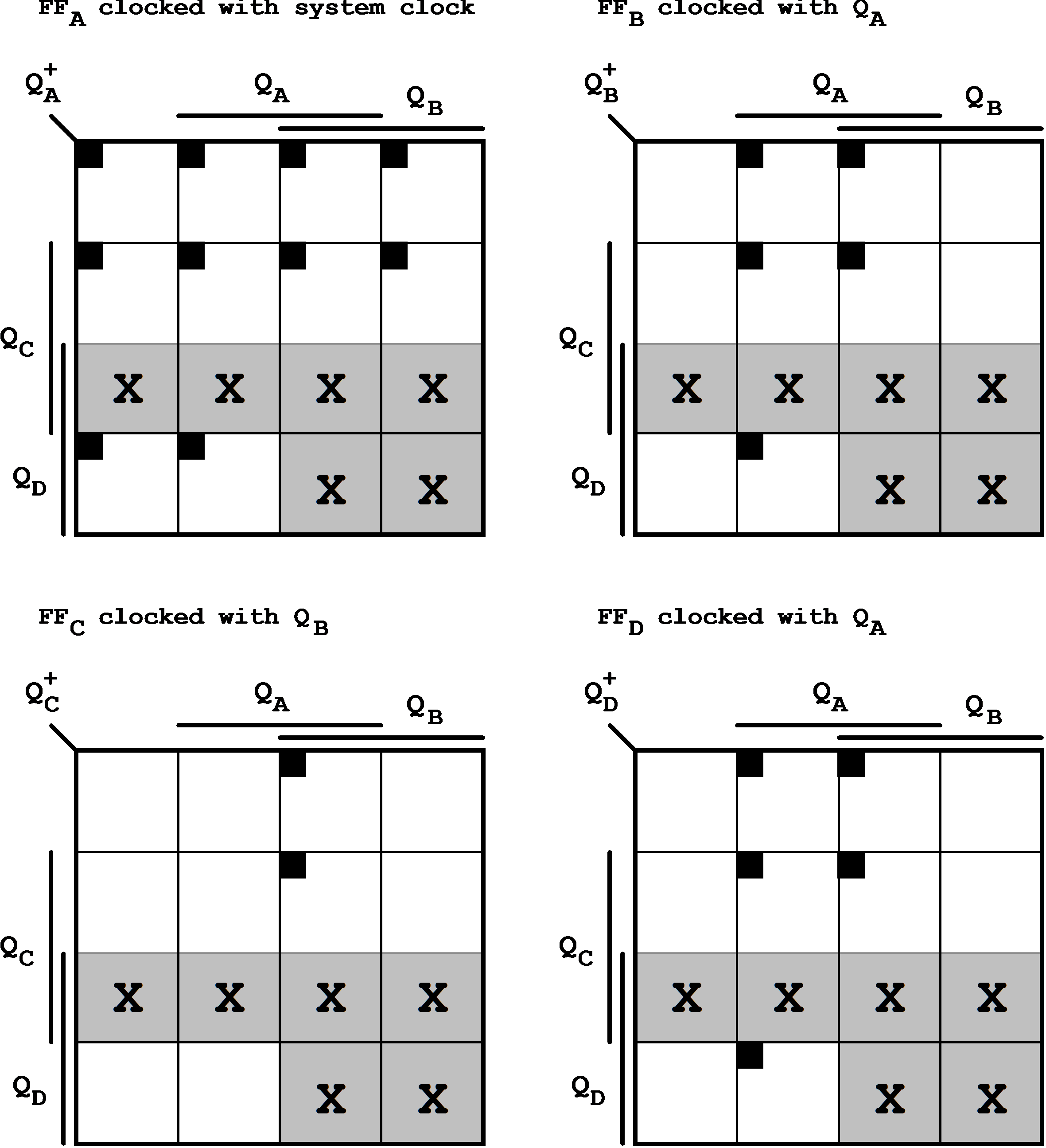
Figure 7.16: Application diagrams of the BCD counter:
X: "don't-care" fields , ■: clocked fields.
Up to this point the the design of the asynchronous BCD counter has been flip-flop independent. In the next step the flip-flop controls have to be entered again. In the example this will be done for a realization using D flip-flops (Fig. 7.17)
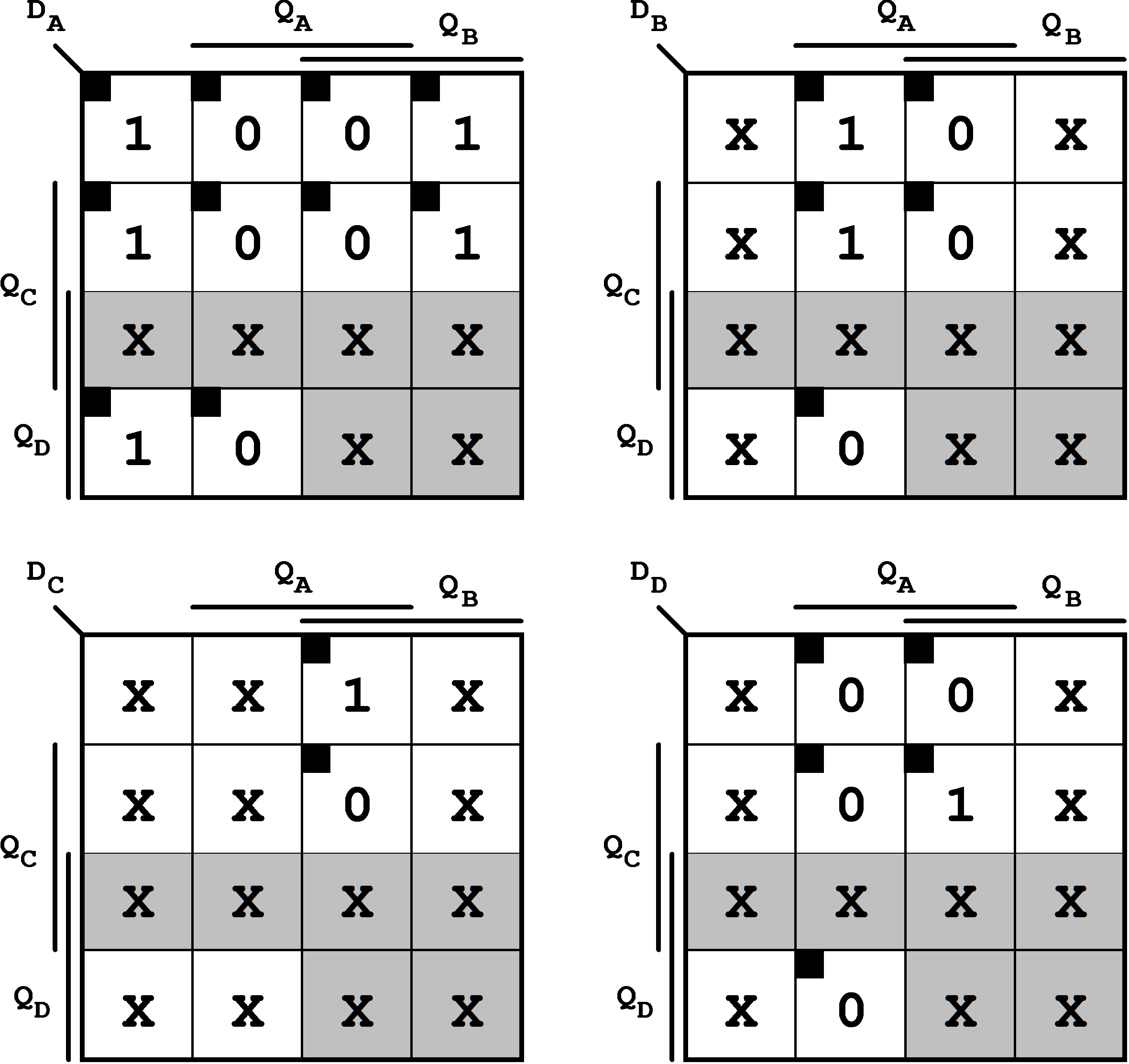
Figure 7.17: Application Diagram of the BCD Counter (for D FF Realization).
Forming adequate implicants leads to the following equations for the flip-flop inputs:
 | (7.8) |
This results in the following circuit implementation:
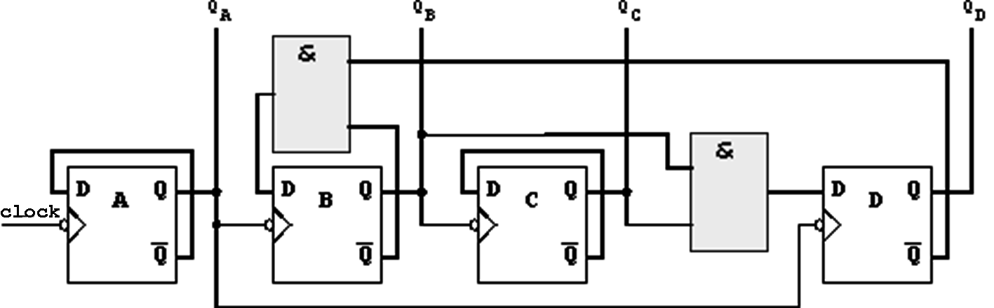
Figure 7.18: Asynchronous BCD Counter.
In summary the phases that lead to a asynchronous counter can be described as follows:
Multi-stage counters can easily be build up using a cascade of individual counter stages. A corresponding principle has already been mentioned during the general description and classification of counters.
Using the example of the asynchronous BCD counter, this method which is very important for practical applications can be described.
To begin with, the individual counting stage will (not according to standard) will be described using a simple equivalent circuit.
| Figure 7.19: Circuit Symbol (not according to standard) of a BCD counter. |
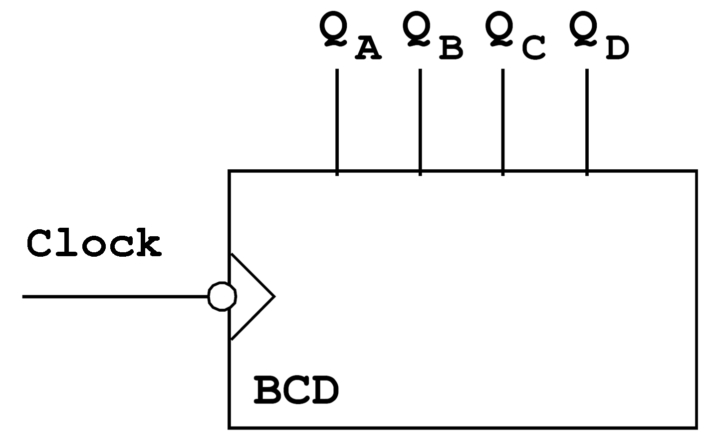 |
The counter described with this symbol represents one counter decade (tetrade), i.e. the counter range is 0 to 9. When larger counting ranges have to be covered, the corresponding number of counters (decades) has to be cascaded.
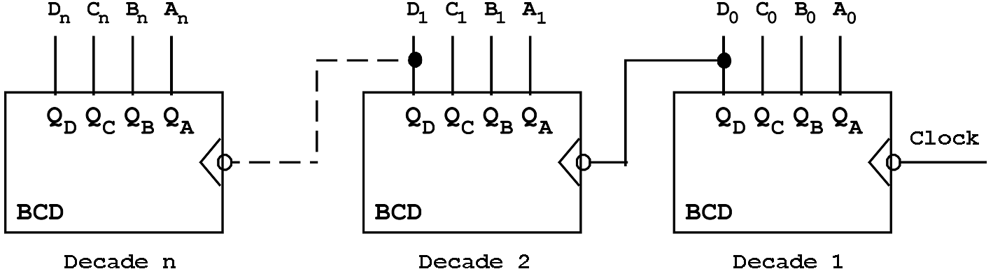
The most significant output QD of each decade is connected to the clock input of the next counter.
Example:
A three-digit BCD counter (three decade) has a counting range from '000' to '999'.
| Contents | Previous Chapter | Next Chapter |